

HDI Circuit Board Technology
The main advantage of these circuit boards is that they can be made much smaller than non-HDI ones. This is vital in many applications, including medical devices, where small sizes are essential. For example, a pacemaker or other device needs to fit inside the human body and must still be capable of transmitting high-speed signals.
These hdi circuit boards also tend to have longer lifespans than traditional designs. This is due to their ability to handle stress from temperature and pressure better. They can also resist damage from physical impacts, which is particularly important for industrial use. These features can help make the boards more cost-effective and durable.
Another key benefit is that these boards are easier to assemble. This is because they do not have as many vias. As a result, the circuit board can be manufactured faster and at lower cost. This can make them a viable option for a variety of industries and applications.
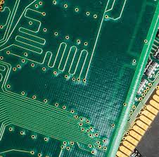
How Does HDI Circuit Board Technology Impact PCB Design?
The use of HDI circuit boards is growing across the globe. They are used in various electronic devices, including mobile /cellular phones, touch-screen devices, laptop computers, digital cameras, 4/5G network communications, and military applications, such as avionics and smart munitions. The technology is also used in wearable devices, such as fitness trackers and smartwatches.
One of the major challenges for the industry is balancing component density and signal integrity. This requires the use of shortest trace lengths, consistent impedance paths, sufficient ground planes, and isolation of digital, analog, and power signals. It also involves selecting the best materials for the different layers of the PCB and incorporating the latest via fill technology into the process.
Some of the newer technologies include via-in-pad, which allows designers to place a via on the surface of a flat land pad. The via is then filled with a conductive material, capped, and plated. This can help to reduce overall etching times and reduce parasitic loads. It can also be used to improve the signal transmission path and decrease cross delays.
The latest HDI PCBs are available in a variety of configurations. Some are 1+N+1, while others have 2+N+2 or 3+N+3 build-up layers. Some have microvias that are laser-drilled and have a diameter of 50 microns or less. They can also feature staggered or stacked microvias. The thinner dielectrics used with these microvias can aid in thermal management.
These PCBs are also capable of supporting a wide range of connectors. The technology can be used for a number of types of interconnects, including copper wires, multi-layer coaxial connectors, and hybrid connectors. They can also be used for signal interconnections, such as RF, optical, and high-speed digital.
The process of creating an HDI PCB starts with a stack-up analysis, which determines how many layers to use in the design. The board’s layers should be arranged to accommodate the most components, while still providing adequate space for routing. A good way to do this is by using an HDI layout template. The layout template provides information about the layers that are needed and how to route them. It can also be a great tool to help you calculate the required thickness of your board.


